

Researchers from IBM Research, SUNY Polytechnic Institute’s Colleges of Nanotech Science + Engineering and partners including GlobalFoundries and Samsung have produced advances that will enable the semiconductor industry to pack about twice as many transistors on the chips that power everything from data-crunching servers to mobile devices.
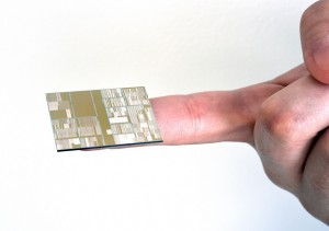
The researchers announced that they produced the semiconductor industry’s first 7nm (nanometer) node test chips with functioning transistors. This breakthrough could result in the ability to place more than 20 billion tiny switches on the fingernail-sized chips that power everything from smartphones to spacecraft.
To achieve the higher performance, lower power and scaling benefits promised by 7nm technology, researchers had to bypass conventional semiconductor manufacturing approaches. The implications of their achievement are huge for the computer industry. By making the chips inside computers more powerful and more efficient, IBM and others will be able to produce the next generations of servers and storage systems for cloud computing, big data analytics and cognitive computing.
In recent years, the chip industry has struggled to sustain a torrid pace of semiconductor innovation. IBM has played a critical role in many of these breakthroughs. For example, IBM scientists led the shift from aluminum wiring to copper to improve processing speeds; using Silicon on Insulator technology to reduce power consumption; and using High-k materials to reduce leakage of electrical current.
Microprocessors utilizing 22nm and 14nm technology power today’s servers, cloud data centers and mobile devices, and 10nm technology is well on the way to becoming a mature technology.
 The IBM Research-led alliance achieved close to 50 percent area scaling improvements over today’s most advanced technology, introduced SiGe channel material for transistor performance enhancement at 7nm node geometries, process innovations to stack them below 30nm pitch and full integration of EUV lithography at multiple levels. These techniques and scaling could result in at least a 50 percent power/performance improvement for next generation mainframe and POWER systems that will power the Big Data, cloud and mobile era.
The 7nm node milestone continues IBM’s legacy of historic contributions to silicon and semiconductor innovation. They include the invention or first implementation of the single cell DRAM, the Dennard Scaling Laws, chemically amplified photoresists, copper interconnect wiring, Silicon on Insulator, strained engineering, multi core microprocessors, immersion lithography, high speed SiGe, High-k gate dielectrics, embedded DRAM, 3D chip stacking and Air gap insulators.
Looking ahead, there’s no clear path to extend the life of the silicon semiconductor further into the future. The next major wave of progress, the 5 nm node, will be even more challenging than the 7 nm node has been.
IBM has committed to spending $3 billion on chip research and development aimed at further extending today’s mainstream semiconductor technologies even while we’re exploring innovations that depart radically from the use of silicon as a primary material in semiconductors and the use of transistors for processing data. They are targeting new kinds of materials and technologies such as silicon photonics, carbon nanotubes and graphene; as well as entirely new approaches to computing, including neuromorphic computing and quantum computing.